
Episode #58
[058] Industry briefing - EUV The Focal Point
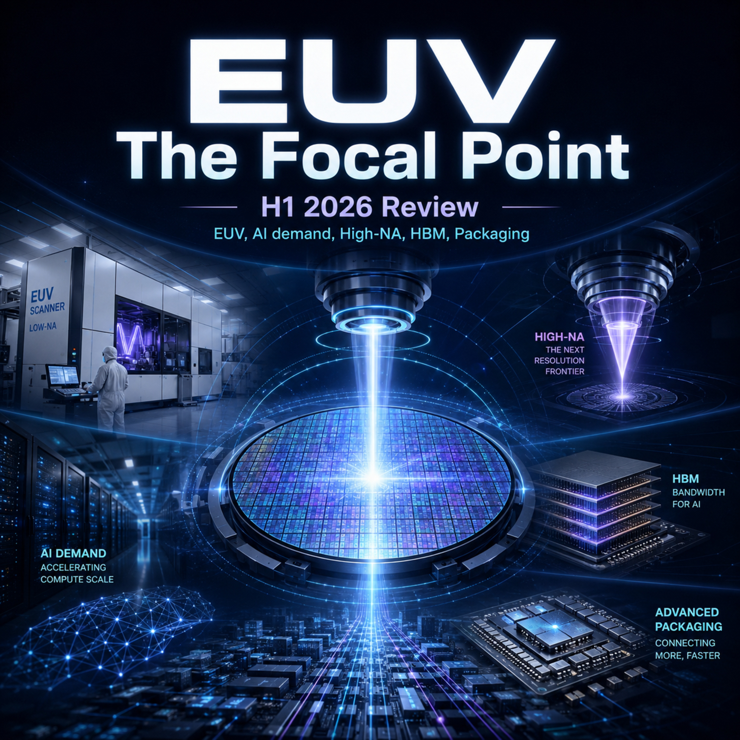
This post was created using AI. Please check the information if you want to use it as a basis for decision-making. Samsung’s revised foundry roadmap puts High-NA EUV around the 1-nanometer-class generation in 2030 while extending the life of its Low-NA EUV platform. At the same time, record equipment spending, new equity financing, and packaging investments show that the economic race is increasingly about sequencing capital across the whole manufacturing system rather than adopting one tool first. Key takeaways - Samsung reportedly moved SF1.4 from a 2027 target to 2029 and plans High-NA EUV insertion with its 1-nanometer-class process around 2030. - Samsung’s roadmap implies continued Low-NA EUV use for SF1.4+ while the company concentrates near-term resources on the SF2 family. - Applied Materials reported record fiscal Q3 2026 revenue of $9.12 billion, up 25% year over year, and guided fiscal Q4 revenue to about $10.25 billion, plus or minus $500 million. - Applied Materials raised its calendar-2026 advanced-packaging growth expectation to more than 70%, reinforcing the broader process-equipment signal highlighted in the August 4 outlook. - Intel upsized its common-stock offering from $15 billion to $20 billion and expects approximately $19.7 billion of net proceeds; the company says proceeds may include capital expenditures and working capital. - TSMC approved about $29.44 billion of capital appropriations covering advanced technology, advanced packaging, specialty capacity, fabs, and facility systems. - TSMC and Sony signed a definitive agreement for a next-generation image-sensor joint venture in Kumamoto, with volume production targeted for 2029. - SPIL reportedly broke ground on a nearly NT$100 billion Douliu plant that will add CoWoS capacity, with first-phase operations planned for 2028. - Nanya Technology says it is evaluating potential expansion sites but has not made a decision on reported new fabs in Yunlin and Pingtung. - U.S. policy pressure is increasingly reaching foundries themselves, with lawmakers pushing stricter scrutiny of advanced-chip orders that could indirectly serve sanctioned Chinese firms. Glossary Extreme Ultraviolet (EUV) — Lithography using 13.5-nanometer light for critical patterning at advanced semiconductor nodes. High Numerical Aperture (High-NA) EUV — The newer EUV platform intended for tighter critical-layer patterning and selective future-node insertion. Low Numerical Aperture (Low-NA) EUV — The established 0.33-NA EUV platform used broadly in current advanced logic and memory production. SF2 — Samsung Foundry’s 2-nanometer-class process family. SF1.4 — Samsung Foundry’s 1.4-nanometer-class process generation, now reported for 2029. Intel 14A — Intel Foundry’s next-generation process platform planned after Intel 18A. CoWoS — Chip on Wafer on Substrate, an advanced packaging approach used for large AI accelerators and HBM integration. HBM — High Bandwidth Memory, stacked memory used with advanced AI and high-performance computing processors. DRAM — Dynamic Random-Access Memory, the volatile memory technology underlying mainstream memory products and HBM.